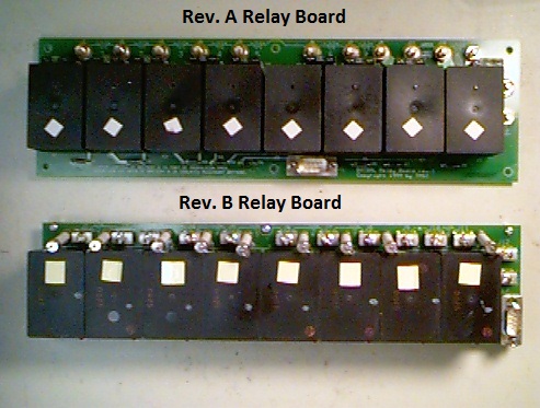
Over time, Lee accumulated a list of improvements to the original design, and designed a new set of Balancer PCBs: Rev B. While there are numerous differnces between the Rev B and Rev A Balancers, probably the two major improvements for Rev B are the ability to handle up to 80 modules (Rev A supported only up to 16 modules without some creative use of the auxiliary control relays to switch between banks of modules), and PCB form factors (L x W) that are compatible with a wider variety of off-the-shelf enclosures.
This is what Lee had to say about Rev B in a 05 Feb 2009 email:
The engineer in me finds it extremely difficult to stop designing and get the damned thing built. When I started, I was just going to make "a few improvements" in the Balancer, and do another run. It's turned out to be a major redesign, with almost no part left untouched.
But, I finally shot the engineer, and am getting it in production. I ordered 5 Control boards, and the parts to assemble them. They are prototypes, to be sure there are no significant errors or problems. If they are OK, I'll order more for everyone.
Here is a rundown on the new design:
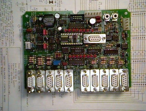
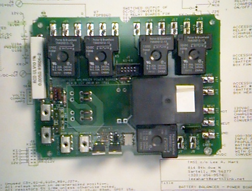
1. Size: The old 12" x 6" Control board has been redesigned as two boards, each 6" x 4.5"; a Control board with the logic, and a Power board with the relays. The two boards stack, to make a pair about 2.5" high. They fit inside a standard 6.5"x5"x3" metal box.
2. Relay board support: The old design had 2 relay board connectors. The new design has 10 Relay board connectors. With 8 cells/batteries each, this supports 80 cells/batteries. You can add more relay boards, but the cabling gets a little more difficult.
3. Switching power supply: The old design had a linear regulator to provide +5v from the car's 12v system. The new design has a switching regulator for this; it reduces 12v power consumption, and supports the faster, higher power versions of the BASIC Stamps without a problem.
4. On-board A/D conversion: The old design used an external multimeter with isolated RS-232 port. The new design has isolated on-board voltage and current measurement circuits. This is where a significant amount of my design time went. It measures from -16v to +16v and from -30a to +30a with 12-bit resolution. In fact, the ranges are set by scaling resistors -- this circuit is intended as the front end for an E-meter replacement project.
5. DC/DC converter control: The old control board had an onboard Vicor Batmod as its DC/DC converter for individual battery charging and balancing, but you could also use an external DC/DC. The new board uses an external DC/DC, but has improved circuitry to control its operation. The A/D converter (#4 above) measures its voltage and current output. An SSR circuit (Solid State Relay) allows the Balancer to switch the DC/DC converter's output on/off, and protect it from battery reversal, over/undervoltage, or overloads. The SSR also insure zero-current switching for the relays, extending their life.
The Balancer also controls power into the DC/DC converter (off, AC line power, DC pack power). It includes inrush current limiting, since many cheap DC/DC converters that people use do not have such protection.
The Balancer can also send commands to the DC/DC to control its voltage and current; either serial data or by using the auxiliary relays to switch setpoints.
Note: My intention is to design a generic DC/DC converter that can be used in any EV, with or without the Balancer. But I don't want to hold this project up any longer waiting for it.
6. Auxiliary relays: There are now 4 (versus 3) auxiliary relays on the Power board. They can be used to switch anything you like; chargers, battery heaters, fans, etc. Each has SPDT 240vac or 30vdc 20amp contacts.
7. EVIBus: There are two EVI (Electric Vehicle Instrumentation Bus) connectors. They can exchange serial data with similarly equipped devices. At present, this is of limited use as few products use EVIbus, and each has its own software peculiarities. But it can also be used with an EVIbus-to-RS232 adapter for an additional serial port.
8. RS-232 serial port: There is a PC compatible RS-232 port, for connecting a laptop or other standard computer, for programming, data logging, or more sophisticated displays or controls.
9. Two Temperature sensing inputs: Same as old board. These can be used to sense the temperature of batteries, motors, interior temperature, etc.
10. HV Input: Same as old board, but lower power and has a wider input voltage range. It allows the Balancer to sense the presence of an AC or DC voltage from 6v to 300v. For example, so it can tell when AC power is present, to use it for heating or charging.
Of course, since then the design has evolved further; in a 21 Mar 2010 email, Lee explains:
Changes from the last revision:
Changed R36 and R37 from 121k to 182k, and R1 (on Power board) from 121k to 150 ohms. This eliminated the V/F voltage shift when reading negative voltages due to the loading of the reverse battery polarity detect circuit (D44, U16, Q6, and R10).
Changed control of the DC/DC output solid state relay (K8) from shift shift register U2's QA output to BASIC Stamp P15. This allows the DC/DC to be switched on/off at will by the software.
The two MOSFETs in the solid state relay (K8) on the Power board were wired in series instead of parallel. This way, they block current in both directions when off, to protect the DC/DC converter in case it or a pack battery is connected backwards. Larger MOSFETs with lower Rds(on) are used to keep their voltage drop low.
Q9, D1, and R7 were added to the Power board. If either the battery is backwards (and the reverse-polarity relay hasn't corrected it), or the DC/DC is connected backwards, their minus side will be more positive, which turns on Q9 to short the MOSFETs gate to their source holding them off.
Added D47, a bidirectional zener to clamp the V/F voltage input range to about +/-18v. This prevents a large negative voltage from causing the V/F converter to output a false frequency that looks like a more positive voltage.
Added D48, a germanium diode to clamp the I/F current input negative range to about -50 amps. This prevents a large negative current from causing the I/F converter to output a false frequency that looks like a more positive current.
As part of this change, R2 on the Power board was changed from 1.3k to 150 ohms, and R56 and R57 were changed from 1.3k to 1.87k. The germanium diode conducts at 0.25v, with -50a in the shunt (R5).
Changed diode D41 to an LED labeled "TEST". It can be turned on and off with BASIC Stamp P12 under software control as a test light, without affecting any other outputs.
And then on 11 Apr 2010:
Attached please find an update on the CONTROL board schematic. It's the same as the one I sent you a week or two ago, except that I changed the optocouplers for the EVIbus interface. The receive opto was changed from a 4N35 (6-pin) to a 6N139 (8-pin) for receive. The transmit opto was changed from a 4N35 (6-pin) to a PC817 (4-pin) to make room.
This was at John Lussmyer's urging. The 4N35 *usually* works, but we're using it at 0.5ma and its CTR is spec'd at 5ma. This led to large variations in the speed of parts. Switching to other optos that were spec'd at 0.5ma or 1ma fixed the variations, but then they were *all* slow.
The 6N139 is a more expensive part, but is spec'd for both 0.5ma and high speed.
Revision History:
18 Feb 2012: Added links to assembled PCB images.
01 May 2010: Updated with descriptions of design changes since Feb 2009.
06 Sep 2009: Relocated Rev A information elsewhere.
05 Apr 2009: Updated with Rev B information.
22 Sep 2002: Added links to bare PCB images.
05 Aug 2002: Initial revision.